|
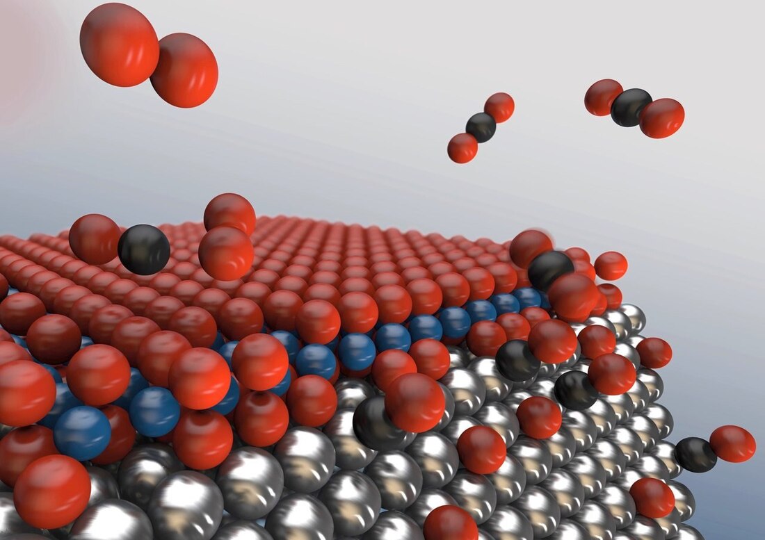
A Precise Artistry: Exploring the Marvels of Atomic Layer Deposition Welcome to the realm of advanced surface engineering, where Atomic Layer Deposition (ALD) reigns supreme. With its exceptional precision and control, ALD has revolutionized the field of thin film deposition. In this article, we will take a captivating journey into the intricacies of ALD, uncovering its extraordinary potential in surface coating and beyond. Building Blocks of Excellence: Understanding Atomic Layer Deposition Process and Equipment At the core of ALD lies an ingenious process that enables the controlled growth of atomically thin layers on various substrates. By precisely introducing ALD precursors in a sequential manner, each atom layer is deposited with unparalleled accuracy. To facilitate this precise dance of atoms, specialized ALD equipment is utilized, ensuring the optimal conditions for deposition and achieving remarkable uniformity. Unleashing Innovation: Exploring the Vast Landscape of ALD Applications The applications of ALD span a wide spectrum of industries, where its capabilities have been harnessed to unlock new possibilities. From microelectronics to biomedical devices, ALD has emerged as a versatile technique with countless applications. ALD’s ability to create conformal coatings, modify surface properties, and enhance material performance has paved the way for groundbreaking advancements in electronics, energy storage, catalysis, and more. Materializing Potential: Delving into ALD Materials and Techniques Materializing Potential: Delving into ALD Materials and Techniques ALD offers a rich assortment of materials for thin film deposition, including metal oxides, nitrides, and sulfides, as well as organic compounds. The choice of materials and their precise control during deposition empower scientists and engineers to tailor coatings with specific properties, such as electrical conductivity, optical transparency, or mechanical strength. The synergy between ALD techniques and materials opens new doors for innovation and technological breakthroughs. Unraveling Mysteries: ALD Research and Exploring Growth Mechanisms In the pursuit of continuous improvement and innovation, the world of ALD is propelled by research endeavors that seek to unravel the underlying growth mechanisms. Scientists delve into the intricate details of chemical reactions, surface interactions, and film properties to uncover the hidden secrets of ALD. Through collaborations between academia, industry, and research institutions, these discoveries fuel advancements in process optimization, novel precursors, and new ALD approaches. Beyond Conformity: Unveiling the Unique Film Properties Enabled by ALD The precision of ALD results in thin films with exceptional properties that go beyond what traditional deposition techniques can achieve. From excellent uniformity and conformality to controlled porosity and engineered composition, ALD film properties offer a wide range of opportunities in areas such as optics, electronics, and catalysis. The ability to tailor these properties with atomic-level control provides a new paradigm for materials design and development. The Convergence of Science and Nanotechnology The Convergence of Science and Nanotechnology: ALD’s Role in Shaping the Future In the realm of nanotechnology, ALD takes center stage, enabling the creation of nanostructured materials and devices with remarkable precision. By leveraging ALD’s capabilities, researchers and engineers explore the frontiers of ALD nanotechnology, bringing advancements in quantum computing, nanoelectronics, and sensor technologies. The integration of ALD with other emerging fields propels the development of futuristic applications that seemed like science fiction just a few years ago. ALD: Pioneering the Path Forward with Continuous Advancements ALD’s journey is far from over, as researchers, scientists, and industry professionals relentlessly push the boundaries of this transformative technology. Constant advancements in ALD techniques, equipment, and materials expand its capabilities, allowing for even greater precision and versatility. The future holds the promise of thinner films, more complex structures, and applications that will shape our world in ways we are yet to imagine.
0 Comments
 Atomic Layer Deposition (ALD) is a highly precise and controllable thin-film deposition technique that has gained growing attention in recent years. This technique provides highly conformal and uniform thin-film coatings with strict control over film thickness at the nanoscale level. In this article, we will explore the advantages and limitations of Atomic Layer Deposition technology. Advantages of Atomic Layer Deposition Technology One of the primary advantages of ALD technology is its precise, conformal, and uniform nature. ALD coatings have proven to be highly uniform and conformal with precise film thicknesses that are difficult to achieve with other deposition techniques. This accuracy is especially important for the production of electronic devices that require precise and uniform thin-film coatings to ensure consistent and reliable performance. Another advantage of ALD technology is its versatility. ALD is a highly flexible and scalable technique that can be used for a variety of materials and substrates, including metals, semiconductors, and ceramics. Moreover, ALD can be used to deposit a wide range of materials, including metals, oxides, nitrides, and even organic molecules. Another significant advantage of ALD technology is its ability to deposit thin films with excellent properties, such as high purity and crystallinity, at low-temperature conditions. This low-temperature deposition is particularly important for producing thin-film coatings on heat-sensitive materials, such as plastics and polymers, without degrading the substrate. Despite its advantages, ALD technology also has certain limitations, particularly related to the deposition rate and the cost of equipment. The deposition rate is significantly lower compared to other deposition methods, such as Chemical Vapor Deposition (CVD) and Physical Vapor Deposition (PVD), which makes it less attractive for large-scale industrial applications. Another limitation of ALD technology is the cost associated with the equipment. The ALD equipment is expensive, and the process requires high-level technical support and maintenance. As a result, only a few manufacturers produce ALD equipment, making it less widely available compared to other deposition techniques. In summary, Atomic Layer Deposition technology is a highly precise and controllable thin-film deposition technique with a wide range of applications and advantages. Its precise, conformal, and uniform nature and low-temperature deposition are ideal for producing thin films with excellent properties. However, it also has limitations such as a lower deposition rate and high equipment cost. To overcome these limitations, further technological advancements are required. If you want to learn more about ALD technology or other advanced thin-film deposition techniques, visit OkyayTechALD.com. Our team of experts can help you to choose the best deposition technique that suits your needs. Link: https://okyaytechald.com/ |
 RSS Feed
